 English
 日本語
日本語 한국의
한국의 中文
中文我拥有超过十年的PCB和PCBA设计、智能控制电路以及生产优化经验。我与全球工程团队紧密合作,致力于提升产品的可靠性、性能和可制造性。我乐于分享实用的见解,使复杂的PCB技术更容易理解。

你要买什么
?



Author
我拥有超过十年的PCB和PCBA设计、智能控制电路以及生产优化经验。我与全球工程团队紧密合作,致力于提升产品的可靠性、性能和可制造性。我乐于分享实用的见解,使复杂的PCB技术更容易理解。
In PCB layout services , smart design choices prevent signal interference, heat issues, and high defect rates in mass production. Here are 10 battle-tested rules to maximize reliability and manufacturability (DFM).
1. Place Bypass Capacitors Near IC Pins
Position bypass capacitors as close as possible to the IC power and ground pins to minimize parasitic inductance and filter out power noise.
2. Maintain Uniform Component Alignment
Align components uniformly and group related functional parts to streamline SMT assembly, reduce placement errors, and speed up AOI inspection.
3. Add Ground Copper Flood Under ICs
Pour copper beneath top-layer ICs on multi-layer boards to improve thermal dissipation and enhance EMI shielding when tied to Ground.
4. Use Standard IPC SMT Pad Lengths
Avoid excessively long SMT pads to prevent surface tension from pulling components off-center (tombstoning) during reflow soldering.
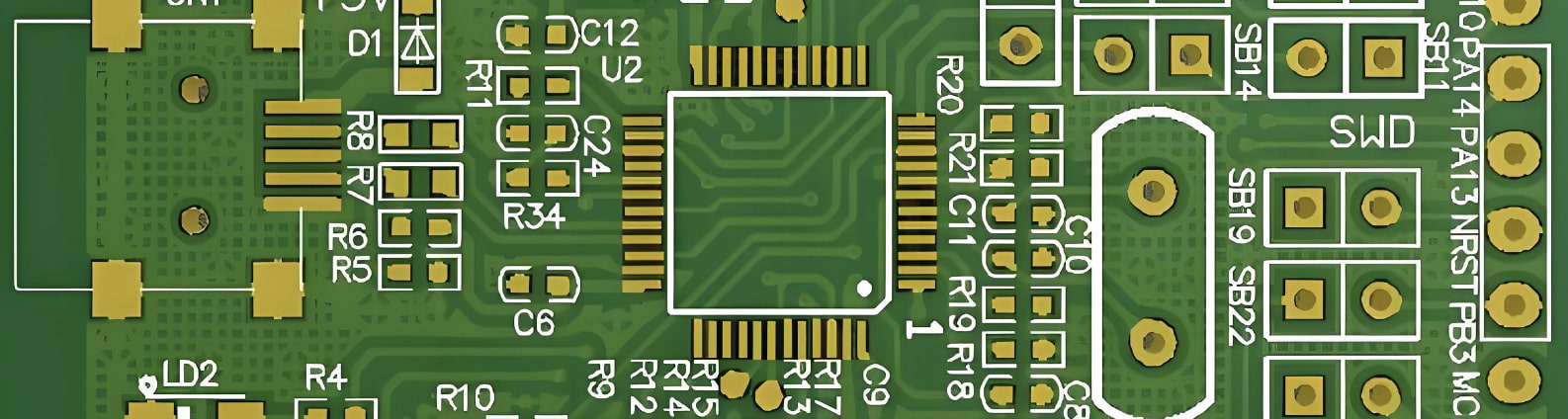
5. Keep Ground Traces Short and Direct
Route ground connections with short, wide traces directly to the GND plane to lower impedance, ground bounce, and radiated noise.
6. Add Solder-Thief Pads for Wave Soldering
Add solder-thief (drag) pads at the trailing edge of narrow-pitch through-hole components to absorb excess solder and prevent bridging shorts.
7. Avoid Vias Directly in SMT Pads
Never place open vias directly on SMT pads, as capillary action will drain solder paste into the via, causing cold or weak solder joints.
8. Avoid 90° Right Angles and Acute Bends
Use 135° (45° chamfered) trace bends instead of sharp 90° or acute angles to maintain impedance consistency, prevent acid traps, and reduce EMI.
9. Add Surge Protection Resistors on Power Inputs
Place a wirewound surge-limiting resistor or TVS device in series with power inputs to absorb voltage spikes and boost circuit immunity.
10. Route Power Lines in Branching Topologies
Distribute power in a "trunk-to-branch" tree layout and avoid closed loop traces, which act as antennas that radiate and pick up noise.
Need Professional PCB Layout Services?
Partnering with an experienced layout team ensures high board performance and seamless transition to mass production.
For more detailed information, please see the link below:
👉 https://www.ruichunpcba.com/product/custom-pcb-layout-services-turnkey-pcb-design-assembly
留言
扫描至 WhatsApp :



 IPv6 网络支持